1, I'm not completely confident on the phase relationships of the traces. I saw numerous differences as I made the measurements. Not sure why.
2, Reference is the schematic by KK6FT and N6QW, fig 7, page 28 of the April 2015 QRP Quarterly. I've uploaded a picture of the schematic here for reference to go along with my scope screen shots. Incidentally, QRP Quarterly is a great magazine for the homebrewer. I highly recommend subscribing to it.
3, Frequency input is 4,914 mhz.
4, 6vdc fed to both circuits and both n/c positions of where RY2 will be are grounded.
First screen shot shows A trace on the bottom and B on top. A is the filter output and B is the output of the toroid T2. No issue here as the voltage out is about 1/2 of what is fed into it.


Here I'm looking at the output of the first toroid T1 to the 39pf cap on A and B is looking at the input of the xtal. Again the distortion is cleaned up a little through the cap.

The 4th picture shows the input to the board from the signal generator. This was a surprise as I expected a nice looking sine wave.

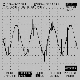
Next up is the signal generator output, but not connected to the board. I wanted to make sure how the signal looked in case it was the board having some effect.

Finally a shot of the board's output depicting how it was processing the signal. Looking at it I'm not sure I really am happy with the results.

Up for discussion:
1, Why is the input signal being distorted by the circuit? Is it due to an impedance mismatch? I did try various levels with no change in behavior.
2, The signal is cleaned up completely after the first crystal. I'm glad it happened but I did not expect the filter would have to do this. I thought it's only function in life was to reject all but the band pass frequencies.
3, The signal looks fine coming out of T2 and at the base of the 2N3904. After that its a mess and you can see the output after the 100nf cap.
4, Construction of the board is me-squares style etched into a board. I suppose its a bit of a mess and is this contributing factor? i don't think so but since I was treating this a prototype board I was not all that concerned. There was not too much thought put into the layout, just follow the schematic and solder. So there would be room for improvement in a finial version.
5, I did play a little with the supply voltage. I varied it between 5 to about 6.2 or so while watching the output signal. My thinking was where in the characteristic curve of the transistor was the signal operating? I was curious to see if the quality of the signal improved or not. It did not.
6, Input from the signal generator varied from about 50mv up to around 300 to see the effect. Nothing to really note as it was done quickly to see if that was an issue. The screen shots were taken with the sig gen set at 100mv. A more detailed investigation will be done here once I know what the output of the previous stage in the LBS project is known.
7, I think I need to investigate further the 2nd amplifier. I'm not confident its working correctly. I am not getting a signal I expected on the collector of the 2N3904. 1volt signal, clean, is on the base and 40mv with hash on the collector.
8, Even though testing of the xtall filter showed a bandwidth of of about 1,500hz, I noticed when adjusting the frequency of the input, it appeared to be passing far more. In fact a great deal more. At least a meg. Now it was quick changes to see the effect and I didn't take any measurements, yet. But while varying the signal in 4 steps, 4.913, 914, 915, and 916, the output signal did not vary much if at all with 4.914 or 4.916. Again crude adjustments done quickly and a more detailed look is needed.
9, I covered a lot of ground and discovered I left out 2 caps, installed connectors and jumpers, bad dc jack, forgetting an important step in the setting up the signal generator, and more than a few scope issues. Long day at the bench and could have overlooked something easily. So be gentile if there are any comments, (hihi) hope there are, and look forward to any suggestions or ideas.
For those of you who know, beware, this is only a preamble to the thesis. hihi.
73, Peter
The sine wave looks like there is noise on it (layout issue? shielding? missing caps?)
ReplyDelete73 Gord
I see 2 things with the output Gord. First is the noise and 2nd is no amplification. I'm only getting about 40mv out. Caps are there, so I'm leaning towards layout although that doesn't explain the output level. So I'm in the process of making a temp. 3904 amplifier on a separate board and will re-direct the output of T2 to it and hopefully see improved results.
DeleteHow's your board coming along?
73, Peter